Revolutionizing Optical Responses: Reflectance Measurements for Metasurface Wafer Technology
- On August 1, 2024 TAGS: 410-DHR, emittance control, infrared materials, metasurfaces
As we push the envelope to devise creative solutions to global problems, researchers have concentrated their efforts on the emerging field of metasurfaces. A metasurface is an engineered two-dimensional material designed to manipulate electromagnetic waves, such as light, in ways that are not possible with natural materials. These surfaces consist of arrays of subwavelength structures, known as meta-atoms, that can be tailored to exhibit specific optical properties.
By carefully designing the shape, size, and arrangement of these meta-atoms, metasurfaces can control wavefronts, polarization, and phase of light, enabling applications like thermal control, advanced imaging, holography, optical communications, and efficient energy harvesting.
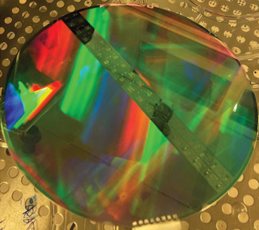
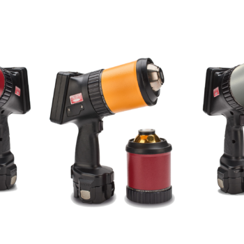
Sun et al. (2022) from the University of Southampton applied these principles to manipulate the optical properties of a silicon wafer with an aluminum-doped zinc oxide metasurface. Specifically, they modified the infrared (IR) reflectance in the mid-wave infrared (MWIR, 3-5 μm) and long-wave infrared (LWIR, 8-13 μm) bands. This analysis was conducted using a benchtop Fourier Transform Infrared Spectrometer (FTIR) and the SOC410-DHR, a portable handheld directional hemispherical reflectometer from Surface Optics Corp.
The SOC410-DHR demonstrated agreement with the benchtop FTIR, allowing the research team to rapidly test several positions on the wafer to identify areas of metasurface uniformity (Figure 1a-b). They also input reflectance data from multiple angles of incidence to build a simulation model of mid-wave and long-wave reflectance as a function of incidence angle (Figure 1c). These simulations were used to predict further manipulations of the surface reflectance to achieve the desired optical properties for a wide range of applications.

Figure 1. a) Thermal (LWIR) image of the metasurface with gradient exposure dose and 5 nm Ti. b) Experimental directional hemispherical reflectance (DHR) of the wafer in (a). c) Experimental (dots) and simulated (lines) MWIR and LWIR reflectivities of position 5 against different incident angles θ.
The full article is open source and can be found here: https://doi.org/10.1002/adom.202200452
For more information about our IR reflectance and emittance measurements, reach out to djacobsen@surfaceoptics.com


0 Comments